A lot has happened since I “finished” the power supply I plan to use for The Laser Project. This is the version I proclaimed success on:

Revision 1 board
But as I continued to test this board it was obvious “revision 1” wasn’t going to cut it. There was excessive switching noise at higher currents. Enough noise that I would get errors reading from the SPI bus and often the supply would just shut down (I’ve never figured out why this is, but an engineer at Maxim Integrated, who makes the control IC for this board, indicated that excessive write errors may cause an abort). So on to revision 2.
Revision 2
Revision 2 was all about noise suppression. I made the following changes:
I moved to shielded inductors. I couldn’t find 6µH shielded inductors in the current capacity I needed, so I changed the circuit to use 4.7µH inductors instead. To do this I doubled the switching frequency, which also reduces the ripple a little bit more.
I add slew control to both high and low side MOSFETs.
I added a snubbing circuit to quench switching noise at the MOSFET drains.
I added a secondary low pass filter to each output to further remove harmonics.
Revision 2 looks like this:

Revision 2 board
This board worked a lot better. Noise was better — there were still some write errors on the bus but I could bring this up to full current without it shutting down. Unfortunately this allowed me to find the next weak spot: heat.
While running one channel on this board to about 30 amps testing a laser diode array, there was a subtle “pop” and no power. The board was hot. So hot that you can “smell” the heat of metal on it. I checked it with a thermal camera and after being off for about 30 seconds the board still read over 300º F. Worse, when power is off to this channel it is sending 8.4 volts out to the laser diode array…which is only supposed to take about 2 volts so the array is likely fried. I buy these arrays used off eBay for a fraction of their list price….but that fraction is still $300, so losing one is pretty heartbreaking.
I tested the bad MOSFET and there was a 12Ω short between source and drain pins, which explains the 8.4v output. Luckily, 12Ω is only .7 amps across the laser diode array, so maybe I didn’t kill it after all. Here’s hoping. What I did kill, however, was the power supply control IC. That channel is toast.
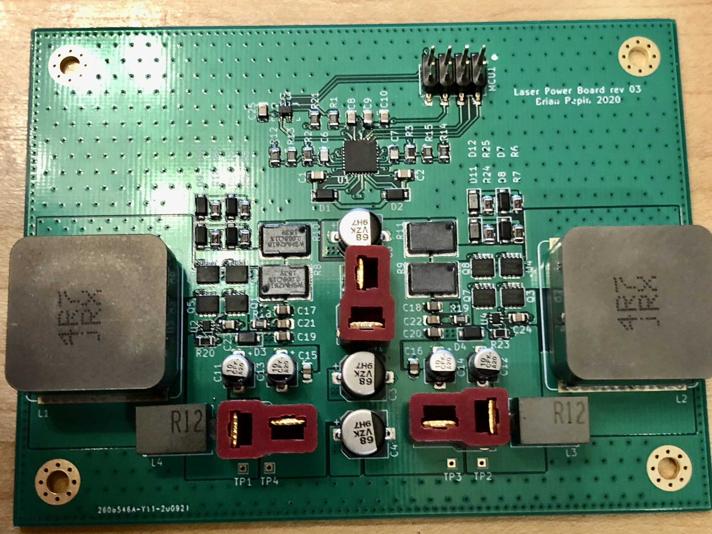
Revision 3
Hey, third time’s a charm, right? I did a bunch of SPICE analysis to simulate this and learned that my circuit is fine. I just need to deal with the heat. I’m using very efficient MOSFETs, but at 1Mhz switching speed and 50 amps…they still get warm.
Math: 11 watts of heat dissipation per channel. Largest dissipation I can expect from the PC board is only about 1 watt.
I am aware that you can run multiple MOSFETs in parallel to reduce power consumption but I never really thought about it here because these single MOSFETs can easily handle the current I’m sending through them. But Ohm’s Law dummy! Power dissipation is:
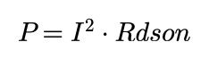
When you run two MOSEFTs in parallel I decreases by half and so does Rdson. The difference is pretty striking: instead of 11 watts per channel for a single MOSFET, running two MOSFETs in parallel only requires 2.8 watts of dissipation (it’s really eight times smaller, but you double the number of transistors so you can only claim a factor of four).
2.8 watts is still over the maximum board dissipation of 1 watt, so I decided to covert the board entirely over to SMD components so the bottom is flat and mounting it on a thermally conductive pad to an aluminum heat sink.
Also, since when the temperature gets high enough clearly bad things happen, I added a circuit that monitors both channels and if they get above 124º C it pulls the reset line of the board low and shuts it down.
All of this required some larger board rework. Lots more components, and switching power supplies need to stay small and tidy to control noise. The result is a few areas of the board are pretty densely packed. Not iPhone motherboard packed, but quite tight for assembling by hand:

Revision 3 has a lot of parts.
Double the MOSFETs, double the gate drive circuitry. Some new glue logic in the upper left to allow the temperature monitors to reset the control IC. The temperature monitors were tricky. I wanted something small because they need to be right next to the MOSFETs. What I got was absolutely minuscule: it’s a scant 1.5mm on its long side and has six pins to connect. Each pin is .2mm wide. You can see them in the photo above as U2 and U4.
I went a little overboard on via stitching. This is a technique to lower noise on the board. But the spacing you need between vias depends on how fast signals are moving on the board. This board is only running at 1MHz. I stuffed enough vias in there to be good well into the GHz range. If I have to do another revision I may remove a few.
I haven’t run this board up to full current yet. The silpad I ordered to transfer heat to my heat sink is back ordered, and because I was assuming I would be using that I actually have less copper surface area on this board than the previous revision. Until that comes in I won’t try to ramp it to full current.
I did test the thermal shutdown by holding a hot air gun over the board and using a thermal camera to monitor its temperature. It trips at 124º perfectly. And I also ran one channel to about 15 amps and monitored its temperature. It is still getting hot, but the temperature increase is slower.
The board also seems less noisy than revision 2. I don’t know if this is due to an overabundance of via stitching or if doubling the MOSFETs affected switching noise. I did recalculate values for the MOSFET snubber circuit, since the MOSFET capacitance doubled. Maybe something good there. Either way scope signals look pretty good even when using the default scope ground lead.
Next Up
Next up I need to do a good burn in with my silpad in place to make sure things don’t get too hot. And speaking of heat, that’s going to be the next thing I tackle for this project. The laser diode arrays will need active cooling. Since I anticipate needing to run them for a while to get the cavity aligned I need to be able to run them safely. So my next step will be a SPI addressable four channel TEC controller. Not as high current, so hopefully fewer revisions and failures.