I needed to revise the power board I’m using for driving the pump laser diodes. The current power board is still a little noisy — it doesn’t work at all if you don’t have an EMI filter on the data bus, and it will stop working if you turn the current up too high. Also, since I designed it I changed how the bus interface connector is going to work. Time for another revision!
Moar Features
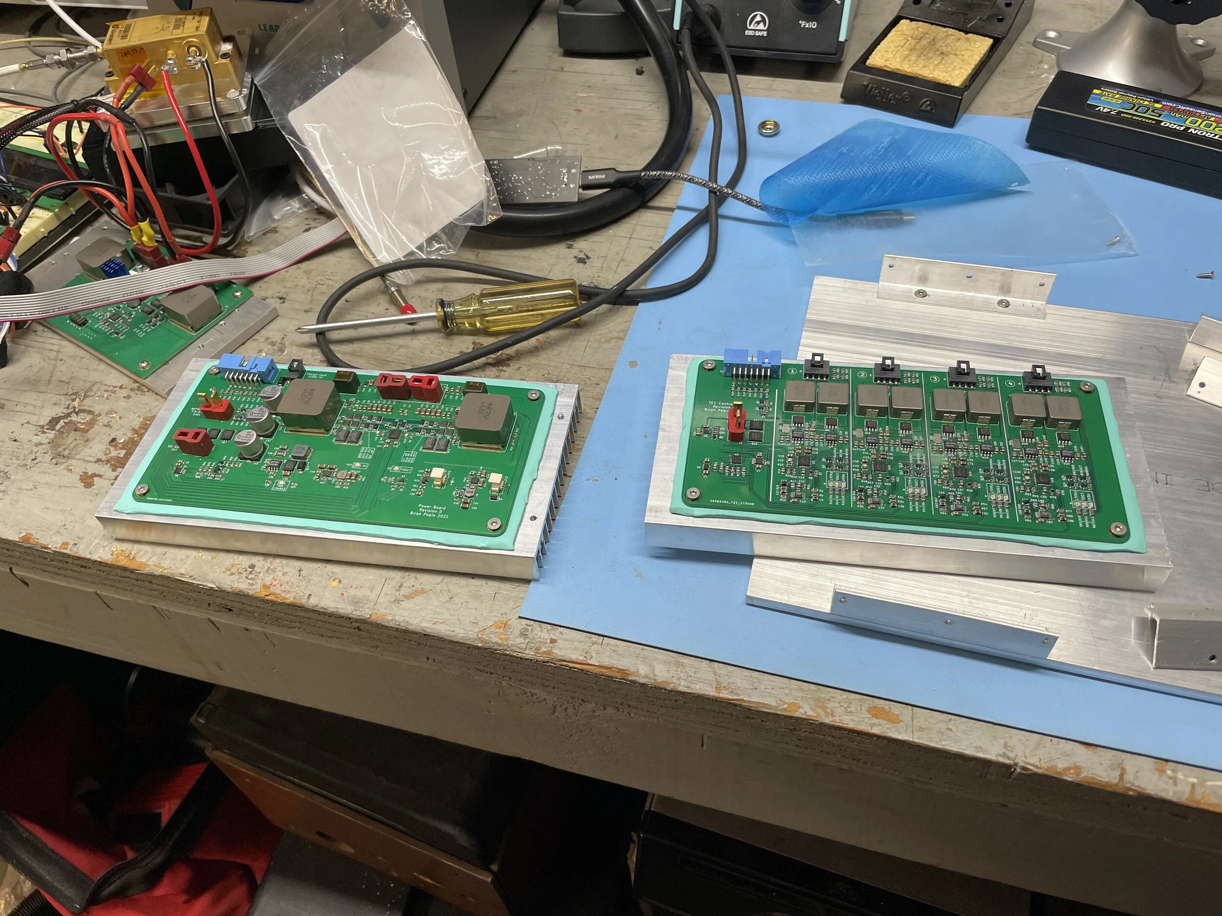
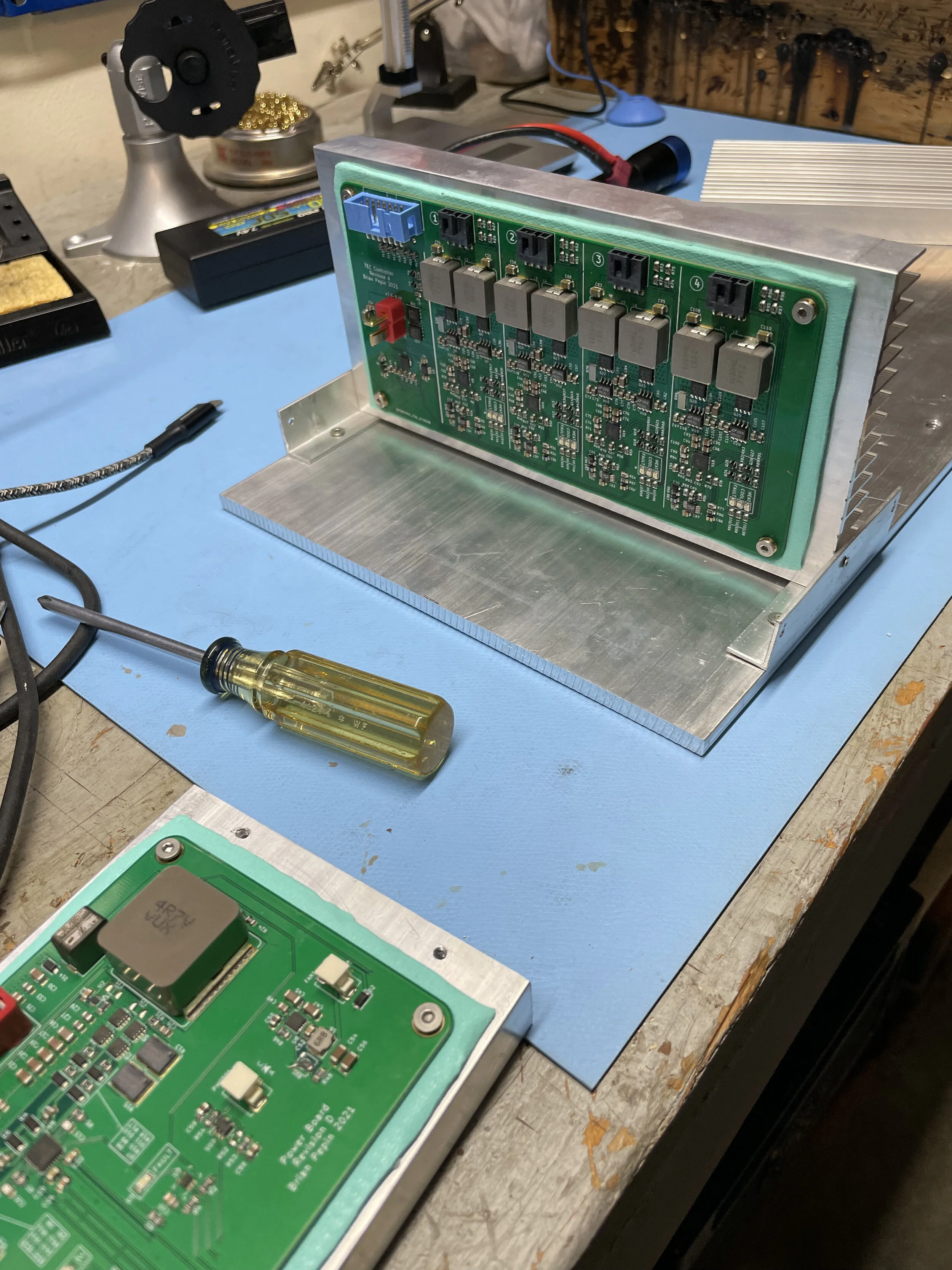
My original goal was to have boards that were about 4” x 3”. But I just couldn't fit the TEC controller on that size board. It has a lot of parts. It’s the first board I’ve created where the component counts for capacitors numbered in the three digits. The larger board size required larger heat sinks and made the power supply quite a bit bigger.
With this new larger board size my power supply layout takes only a small amount of the area. Spreading it out is a bad idea — this layout needs to stay very compact to help control EMI. I was planning a third board and managed to fit all the other stuff I wanted in the extra space. New features:
Power Control - This will take the key switch interlock and controls power to the entire system. A bank of four MOSFETS controls this. I’m also tapping off the voltage drop across the MOSFETSs through Rdson to provide battery current.
Battery Charger - This charges the LiPo cells for the laser and also provides via digital IO the battery voltage and charge status.
Laser Monitor - There will be a photo diode monitoring a faint reflection of the laser output.
Fan Power - A small power supply to power the cooling fan.
3V Power - Main digital 3V power is also supplied here.
Results
The new board came out pretty good:
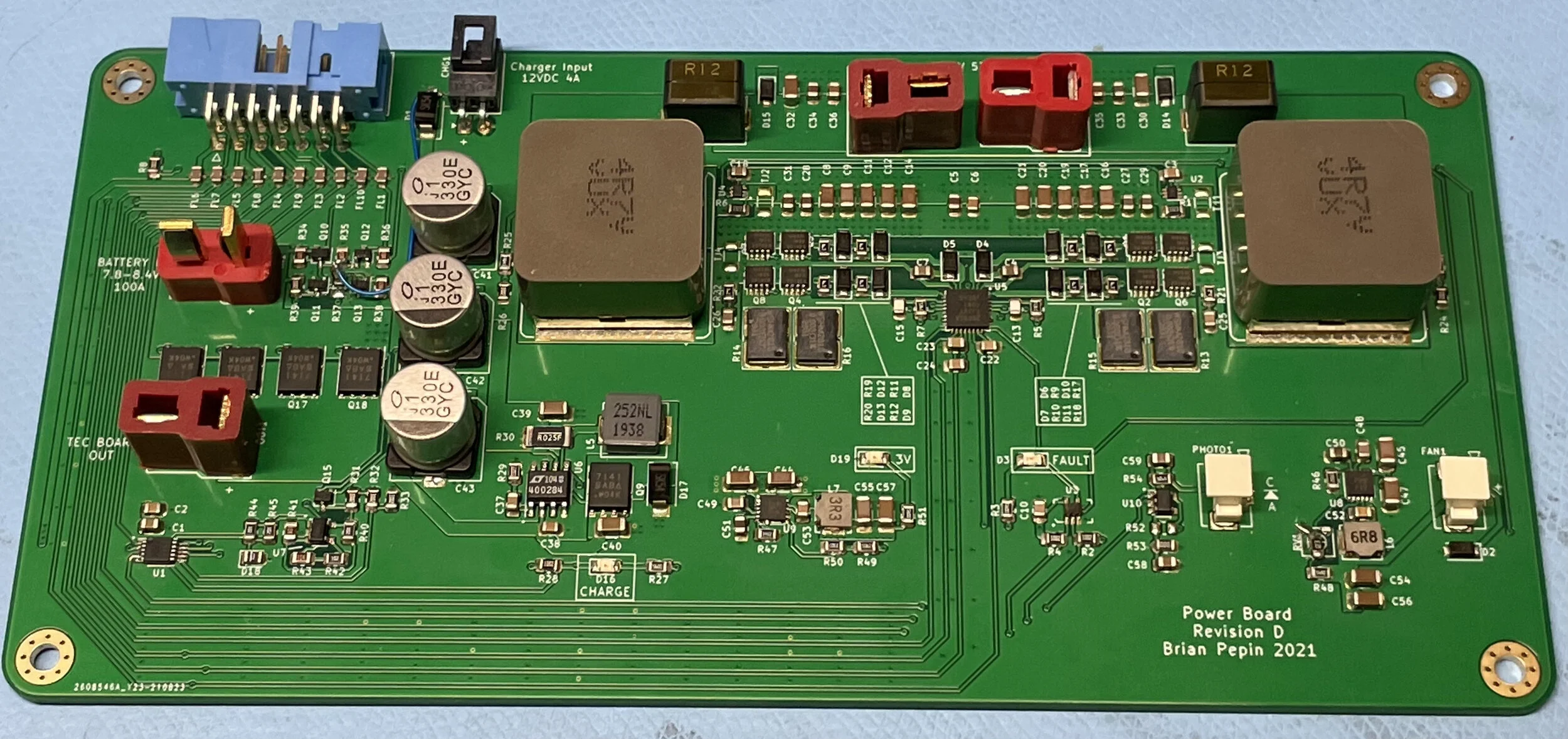
Revison D of the power board
Besides all the new features, there are a lot of things I improved:
Lots more capacitance. I found a great article in IEEE magazine that hinted I might be seriously lacking input capacitance in the old board. I spent a lot of time and math computing needed capacitance for my power requirements. There’s now almost 1500uF of capacitance.
I tightened up the layout of the power section even more and ran heavier traces to the MOSFET gates. The high current loop area is smaller.
All IO traces are isolated from the board and each other by a ground “moat”. I also changed the layer stackup to be Sigal - GND - GND - Signal / Power to keep ground planes close to all signals.
There are 20Mhz EMI filters on every pin if the IO connector.
This board works much better. I no longer need to use an EMI filter around the IO cable, and I can turn the current up and down as fast as I want and the power supply never shuts down (it used to reset when you did that).
All is not perfect though:
I misread the datasheet for the charging IC. It charges fine, but there is a back voltage through its Vin pin that is flowing into the load switch gates and causing the board to stay powered all the time. I fixed this with a bodge wire.
I had to replace the EMI filter on the SCK pin with a jumper. It was tainting the signal. SCK runs at 1Mhz and I don’t have any problems with the other signals, so I don’t know why SCK is special.
It is a mistake to have digital power here. I should have had one of the IO lines be the full battery power with localized power supplies on each board. There is a noticeable voltage droop on the CPU board because of this, and I needed to add some bulk capacitance to the CPU board because the refresh rate of the OLED display was causing some bad voltage drops. I don’t want to respin the TEC board though so I’ll live with it by boosting the voltage a little.
My current monitor doesn’t work. I did the math correctly for how much Op Amp gain I will need for these power MOSFETs, but I made a couple of stupid mistakes: one leg of the differential amplifier flows through another MOSFET and the layout doesn’t use a Kelvin connection to the power MOSFETS.
Oh, and I used the entirely wrong OpAmps. Read the data sheet. The ones I used don’t work at the 3v IO voltage. That’s keeping the laser power monitor from working too.
All that bulk capacitance? Yeah, that’s causing a huge inrush current.
All of that has hopefully been fixed in the new Revision 5. I solved the inrush current problem (I hope) by running the load switch MOSFETs in their linear region during power up to slow the inrush to about 5 amps.
Assembled Unit
While there are some bugs in this board, it works well enough that I can assemble the whole power supply:
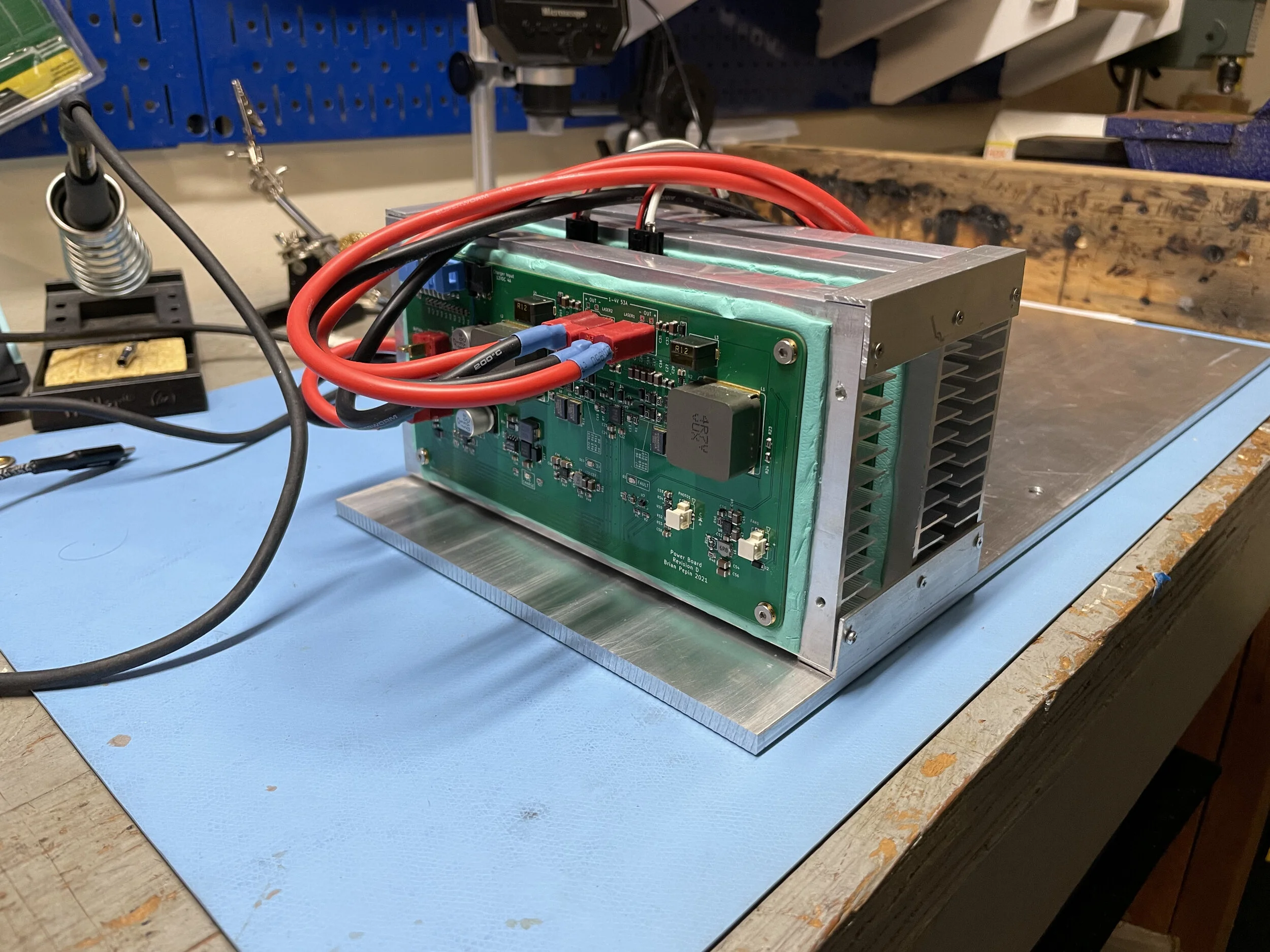

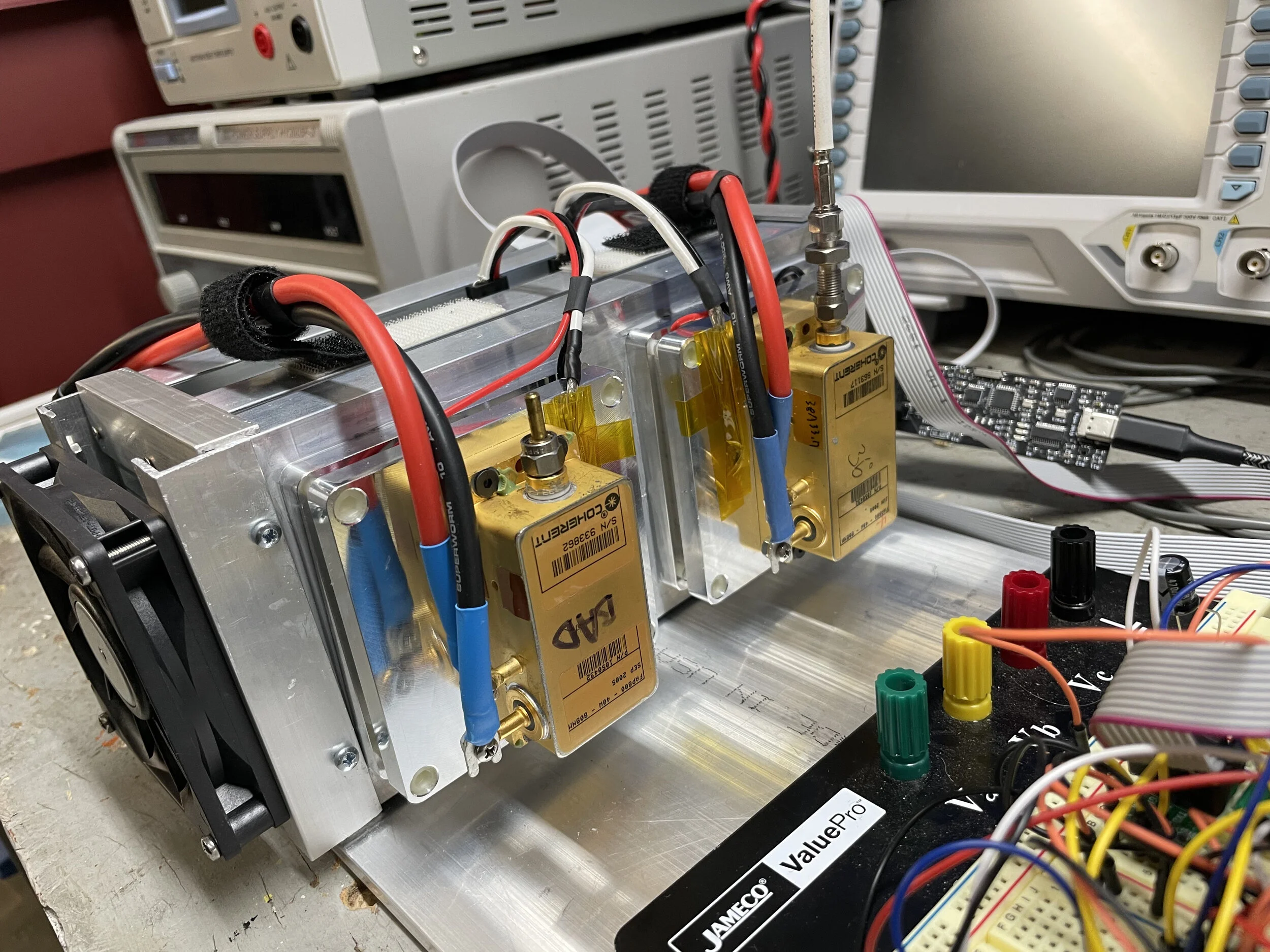
I’m now using this full time and it’s allowed me to go down to a single lab supply (the old boards required three). I can also battery power this but that’s not important yet.